
Package Integrity Testing is required to verify that semiconductor packaging provides adequate mechanical protection, environmental isolation, and long-term reliability throughout the product lifecycle. This testing evaluates the package’s ability to withstand thermal, mechanical, and environmental stresses while maintaining electrical and structural integrity. By identifying defects such as voids, delamination, or seal failures, Package Integrity Testing reduces the risk of premature failure, ensures compliance with industry standards, and supports dependable performance in critical applications.
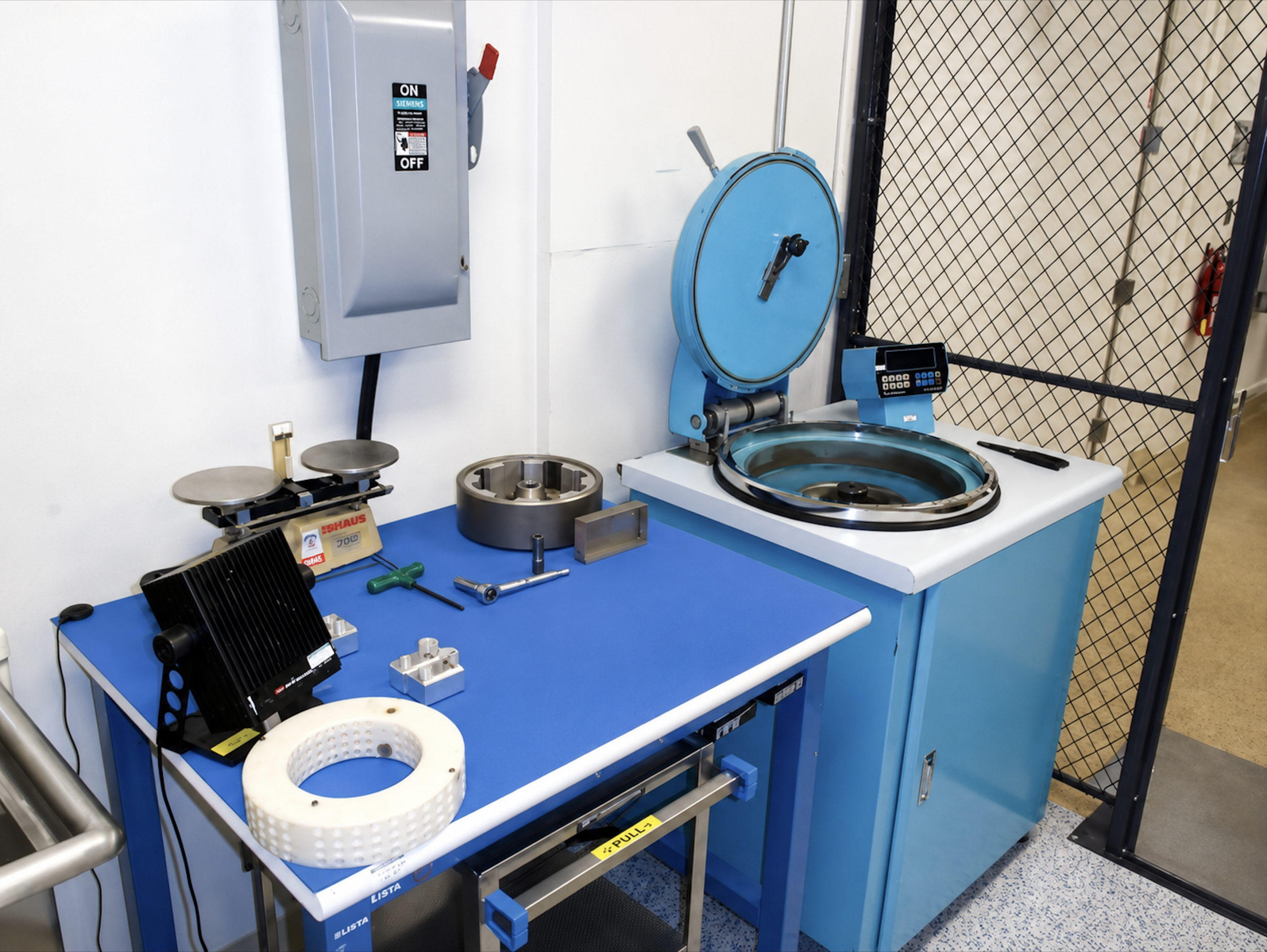

Examples of package integrity testing include constant acceleration and PIND testing (pictured above), as well as additional evaluations such as hermeticity, shock, vibration, and salt atmosphere testing. These mechanical and environmental tests can be followed by electrical testing or visual inspection to ensure the product remains fully functional and compliant with requirements.